 Normal Supply
JESD204B coded serial digital outputs
1.65 W total power per channel at 1 GSPS
SFDR = 85 dBFS (340 MHz),80 dBFS (1 GHz)
SNR = 65.3 dBFS(340 MHz,AIN = −1.0 dBFS);60.5 dBFS(1 GHz,AIN = -1.0 dBFS)
ENOB = 10.8 位(10 MHz)
DNL = ±0.5 LSB
INL = ±2.5 LSB
Noise density = −154 dBFS/Hz at 1 GSPS
DC power supply: 1.25 V, 2.5 V, and 3.3 V
No missing codes
Internal ADC voltage reference
Flexible input range
Programmable termination impedance
400 Ω, 200 Ω, 100 Ω, and 50 Ω differential
2 GHz usable Chiplon input full power bandwidth
95 dB channel isolation/crosstalk
Amplitude detect bits for efficient AGC implementation
2 integrated wideband digital processors per channel
12-bit NCO, up to 4 half-band filters
Differential clock input
Integer clock divide by 1, 2, 4, or 8
Flexible JESD204B lane configurations
Small signal dither
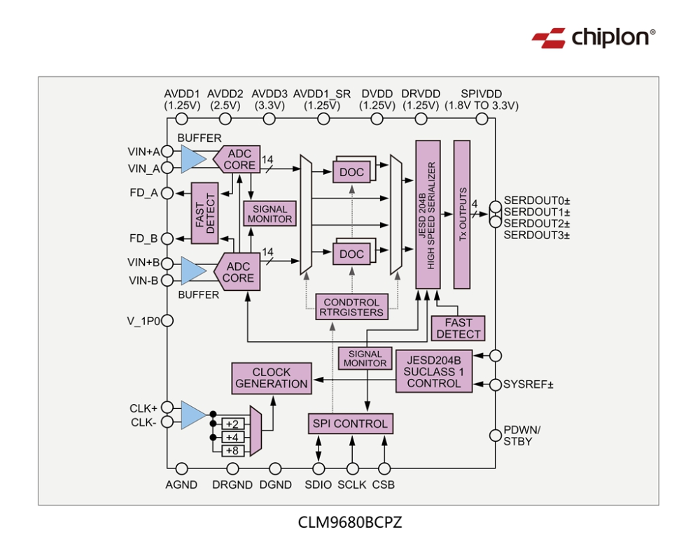
CLM9680E125CS is a dual channel, 14 bit, 1 GSPS analog-to-digital converter (ADC) with built-in on-chip buffer and sample and hold circuit, designed specifically for low power consumption, small size, and ease of use. This device is designed for sampling broadband analog signals up to 2 GHz.CLM9680BCPZ is optimized for wide input bandwidth, high sampling rate, excellent linearity, and low power in a small package. The dual ADC cores feature a multistage, differential pipelined architecture with integrated output error correction logic. Each ADC features wide bandwidth inputs supporting a variety of user-selectable input ranges. An integrated voltage reference eases design considerations. The analog input and clock signal are both differential input signals.Each ADC data output is internally connected to two digital down- converters (DDCs). Each DDC consists of up to five cascaded signal processing stages: a 12-bit frequency translator (NCO), and four half-band decimation filters. The DDCs are bypassed by default.In addition to the DDC blocks, the CLM9680E125CS has several functions that simplify the automatic gain control (AGC) function in the communications receiver. The programmable threshold detector allows monitoring of the incoming signal power using the fast detect output bits of the ADC. If the input signal level exceeds the programmable threshold, the fast detect indicator goes high. Because this threshold indicator has low latency, the user can quickly turn down the system gain to avoid an overrange condition at the ADC input.
JESD204B coded serial digital outputs
1.65 W total power per channel at 1 GSPS
SFDR = 85 dBFS (340 MHz),80 dBFS (1 GHz)
SNR = 65.3 dBFS(340 MHz,AIN = −1.0 dBFS);60.5 dBFS(1 GHz,AIN = -1.0 dBFS)
ENOB = 10.8 位(10 MHz)
DNL = ±0.5 LSB
INL = ±2.5 LSB
Noise density = −154 dBFS/Hz at 1 GSPS
DC power supply: 1.25 V, 2.5 V, and 3.3 V
No missing codes
Internal ADC voltage reference
Flexible input range
Programmable termination impedance
400 Ω, 200 Ω, 100 Ω, and 50 Ω differential
2 GHz usable Chiplon input full power bandwidth
95 dB channel isolation/crosstalk
Amplitude detect bits for efficient AGC implementation
2 integrated wideband digital processors per channel
12-bit NCO, up to 4 half-band filters
Differential clock input
Integer clock divide by 1, 2, 4, or 8
Flexible JESD204B lane configurations
Small signal dither
Communications
Diversity multiband, multimode digital receivers
3G/4G、TD-SCDMA、W-CDMA、GSM、LTE
General purpose software radios
Ultrawideband satellite receivers
Instrumentation
Radars
HFC digital reverse path receivers