 Normal Supply
9 GHz wide input -3 dB bandwidth supports direct RF signal sampling at approximately 5 GHz
Four integrated, broadband extraction filters and NCO modules support multi band receivers
Fast NCO switch enabled through GPIO pin
SPI controls various product features and functions to meet specific system requirements
Programmable fast over range detection and signal monitoring
On-chip temperature diode for system thermal management
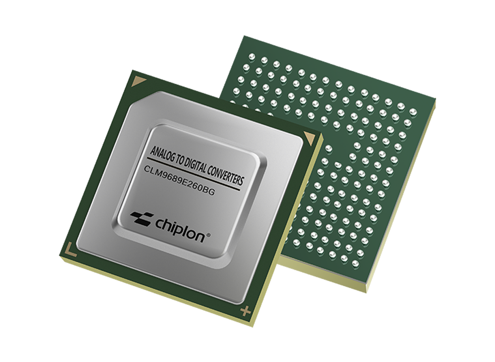
12 mm × 12 mm, 196 pin BGA package
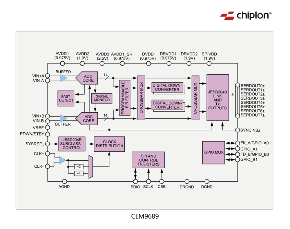
CLM9689E260BG is a dual-channel, 14-bit, 2.6 GSPS analog-to-digital converter (ADC). The device features on-chip buffers and sample-and-hold circuits, and is designed for low power, small size, and ease of use. The product is designed for communication applications and can achieve direct sampling of wideband analog signals up to 5 GHz. The ADC input's -3 dB bandwidth is 9 GHz. CLM9689E260BG is optimized for wide input bandwidth, high sampling rate, excellent linearity, and low power consumption in small packages.The dual-channel ADC core uses a multi-stage, differential pipeline architecture and integrates output error correction logic. Each ADC has a wide input bandwidth and supports user-selectable input ranges.Integrated voltage reference source simplifies design considerations. Analog input and clock signal are differential input signals. The ADC data output is internally connected to four digital downconverters (DDCS) via a crossbar multiplexer. Each DDC consists of a number of cascaded signal processing stages: a 48-bit frequency converter (numerical control oscillator (NCO)) and the extraction rate. NCO can select a preset frequency band within the Universal Input/Output (GPIO) pin range, supporting the selection of up to three frequency bands. The DDC mode of operation of the CLM9689 can be selected through the SPI programmable profile.In addition to the DDC module, CLM9689E260BG also has other functions that can simplify the automatic gain control (AGC) function of communication receivers. By utilizing the fast detection control bit in register 0x0245 of the ADC, a programmable threshold detector can monitor the input signal power. If the input signal level exceeds the programmable threshold, the rapid detection indicator will turn high. Due to the extremely short delay of the threshold indicator, users can quickly reduce the system gain to avoid ADC input overshoot. In addition to fast detection output, CLM9689E260BG also has signal monitoring capability.The signal monitoring module provides additional information for the ADC to digitally process the signal. Users can set the JESD204B subclass 1's high-speed serial output to a variety of single -, dual -, four-channel, and eight-channel configurations, depending on the DDC configuration of the receiving logic device and the acceptable channel rate. SYSREF± and SYNCINB± input pins support multi-device synchronization. The CLM9689E260BG has a flexible turn-off option that dramatically reduces power consumption when needed. All of these features can be programmed through a three-wire serial port interface (SPI). Directly Pin To Pin replaces similar international products without the need to change circuit boards or system software, achieving complete compatibility and replacement. Chiplon Microelectronics has developed its own testing plan to ensure that the factory products meet or even exceed the original specifications, supporting industrial grade working temperatures (-40 ℃~85 ℃).
9 GHz wide input -3 dB bandwidth supports direct RF signal sampling at approximately 5 GHz
Four integrated, broadband extraction filters and NCO modules support multi band receivers
Fast NCO switch enabled through GPIO pin
SPI controls various product features and functions to meet specific system requirements
Programmable fast over range detection and signal monitoring
On-chip temperature diode for system thermal management
12 mm × 12 mm, 196 pin BGA package
Diversity multi band and multi-mode digital receiver
3G/4G, TD-SCDMA, W-CDMA and GSM, LTE, LTE-A
Electronic Testing and Measurement System
Phased array radar and electronic warfare
DOCSIS 3.0 CMTS upstream receiving path
