 Normal Supply
Ensure a lower maximum power supply current within the allowable temperature range
Wide working voltage range: 1.5V to 12V
Tested under 3V conditions, 100% usable
Boost pin (pin 1) is used to increase the switching frequency
The minimum power efficiency is 96%
The minimum open circuit voltage conversion efficiency has been increased to 99%
Improving SCR latch protection
Convert the+5V logic power supply to a ± 5V power supply
Voltage multiplier VOUT=(-) n VIN
Easy to use, only two external non critical passive components are required
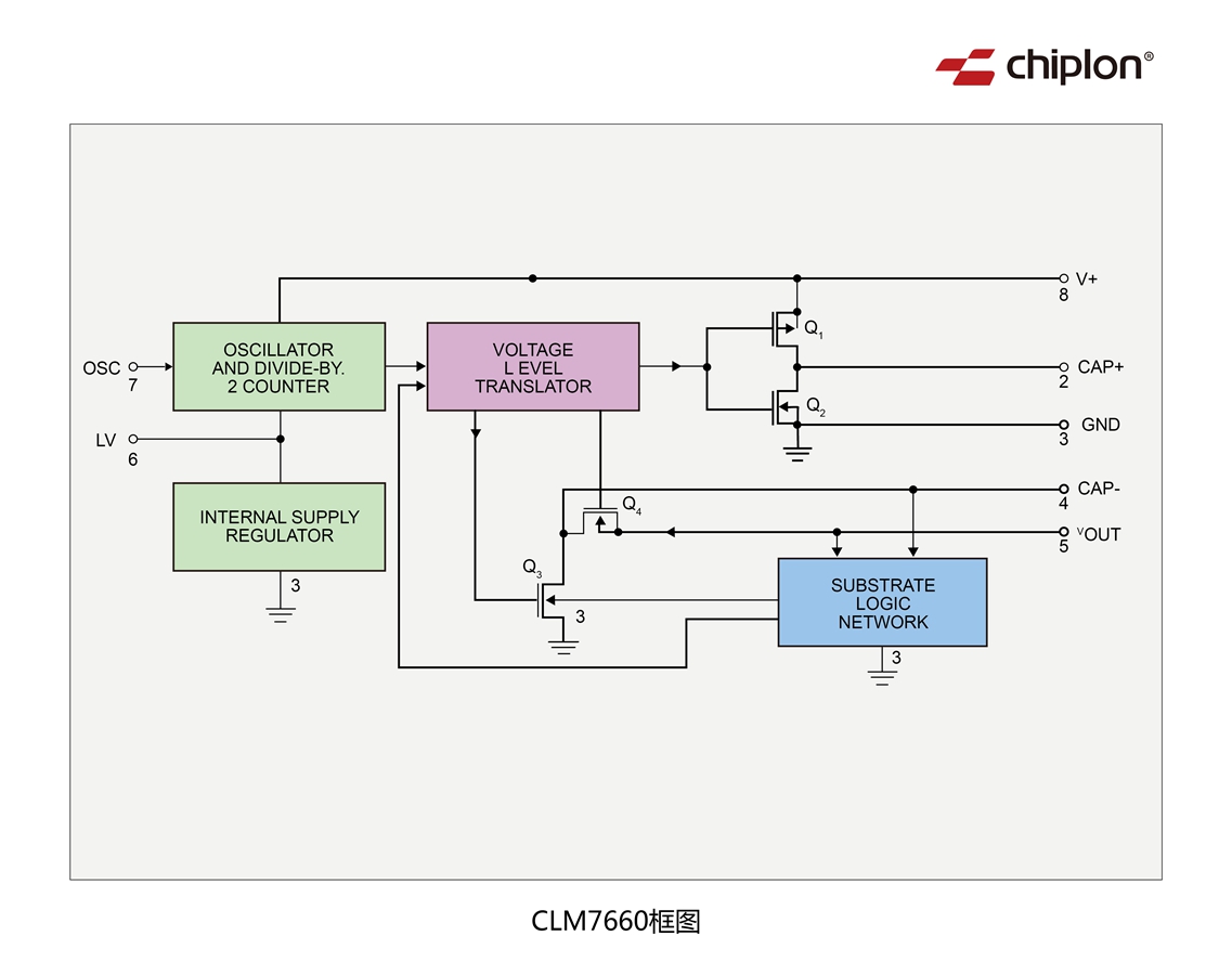
CLM7660SIPAZ is an overvoltage converter that is a single-chip CMOS level conversion integrated circuit. Compared with other similar devices, it has significant performance advantages and extends the working power supply voltage range to 12V, with a lower power supply current. In order to use smaller capacitors to reduce output impedance, the frequency Boost pin is introduced. The CLM7660SIPAZ can convert a positive input voltage ranging from 1.5V to 12V into a negative output voltage ranging from -1.5V to -12V. Only two non critical external capacitors are used for charge pump and charge energy storage functions. CLM7660SIPAZ can be used as a voltage multiplier, and a 12V input voltage can generate an output voltage of up to 22.8V. This chip can also be used as a voltage multiplier or divider. The chip includes a series DC stabilized power supply, RC oscillator, voltage level converter, and four output power MOS switches. The oscillator oscillates at a standard frequency of 10kHz when unloaded, with an input power supply voltage of 5.0V. The frequency can be reduced by adding an external capacitor at the "OSC" end, or by overdriving the oscillator with an external clock. In order to avoid using internal series regulators and improve low-voltage (LV) operation, the "LV" end can be connected to ground. Under medium to high voltage (3.5V to 12V), the LV pins remain floating to prevent device latch. In some applications, an external Schottky diode needs to be connected from VOUT to CAP to ensure latch free operation.
Ensure a lower maximum power supply current within the allowable temperature range
Wide working voltage range: 1.5V to 12V
Tested under 3V conditions, 100% usable
Boost pin (pin 1) is used to increase the switching frequency
The minimum power efficiency is 96%
The minimum open circuit voltage conversion efficiency has been increased to 99%
Improving SCR latch protection
Convert the+5V logic power supply to a ± 5V power supply
Voltage multiplier VOUT=(-) n VIN
Easy to use, only two external non critical passive components are required
Convert+5V power supply to ± 5V power supply
Voltage multiplier VOUT=± n VIN
Provide negative power supply for data collection systems and instruments
RS232 power supply
Voltage divider, VOUT=± VS
